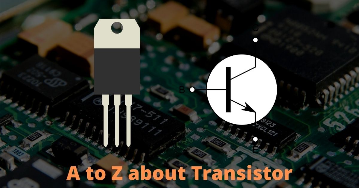
The transistor is the most revolutionary device in the field of technology. You probably read this post either on a mobile or computer or tablet; each of which contains a huge amount of ICs inside them. Many of those ICs consist of a large number of transistors.
What is a Transistor?
If you go through google a little bit, you can find almost a similar definition everywhere. A transistor is a semiconductor device in which a layer of semiconductor is sandwiched between two layers of another type of semiconductor.
Why is this device called ‘Transistor’! Not something else?
The name ‘transistor’ can be referred to ‘Transfer resistor’. It transfers current from a low resistance area to a high resistance area. We will learn the detailed mechanism in the latter part of this post.
Fabrication
- Grown junction technique.
- Alloy junction technique.
- Diffusion technique.
- Epitaxial technique.
Mechanism
A Transistor is two layer of N-type(majority carrier: electron)/P-type(majority carrier: hole) semiconductor in which another type of semiconductor (P-type/N-type) is sandwiched.
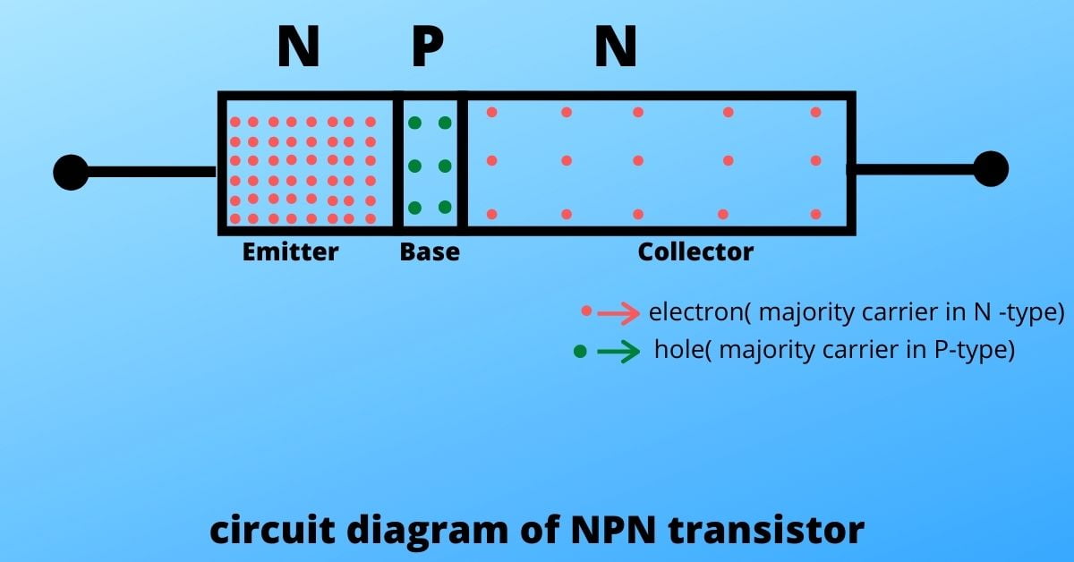
Here P-type semiconductor is sandwiched in between N-type semiconductor. So it is a NPN transistor.
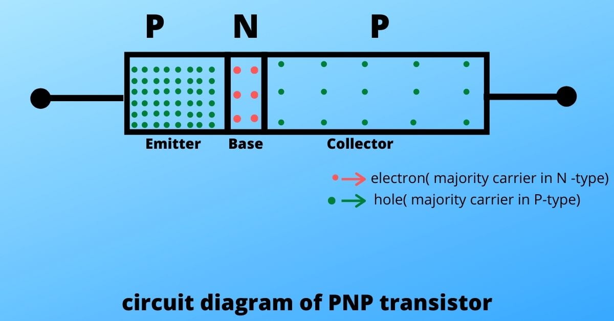
Here N-type is sandwiched in between P-type semiconductor. So it is a PNP one.
In this post, we discuss NPN transistors but don’t worry once you understand the mechanism, it is trivial to understand the PNP . So let’s get started.
To operate an electronic device, first, we need to add a power supply with the device. So if we connect the two ends of a power source then the electrons will be pulled out like shown in the circuit diagram below and we get current flow. Right?
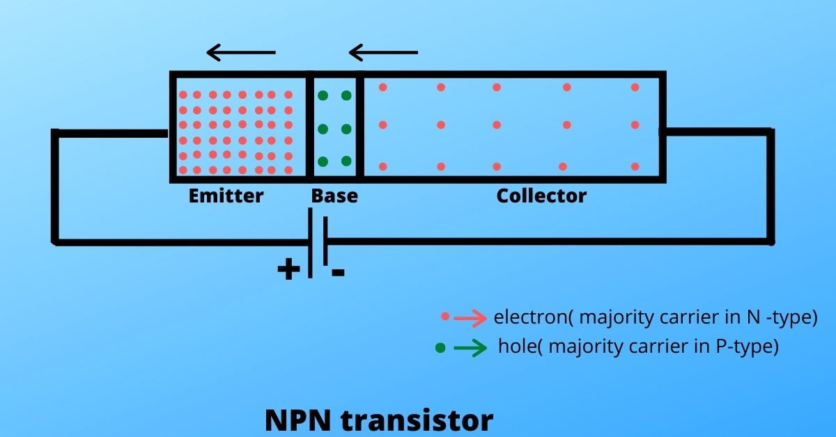
The answer is No. The reason is very simple. As soon as you make a P-N junction, a potential barrier is developed. This barrier resists the flow of electrons from one side to the other side.
Now, to get a current flow through the transistor we need to connect the positive terminal of a power supply to the base junction (for NPN transistor) whose voltage is at least 0.7 volt. Let’s see what will happen after this arrangement.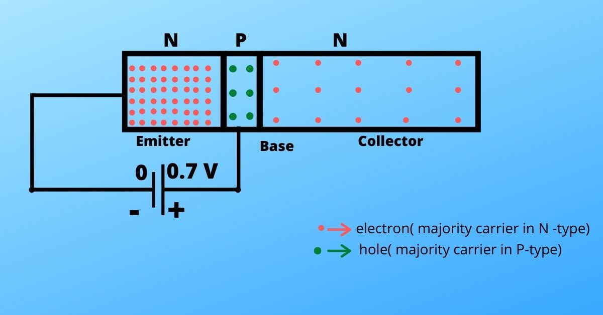
When you connect the base with the positive terminal, the P-side (base) feels a stronger voltage difference than N-side (emitter). So the junction becomes Forward Biased.
As the applied voltage in the P-region is equal or more than 0.7 Volt (for silicon) and the junction is in forward bias, the depletion region vanishes and the electrons from N-side diffuse to P-side and the holes from P-side diffuse to N-side.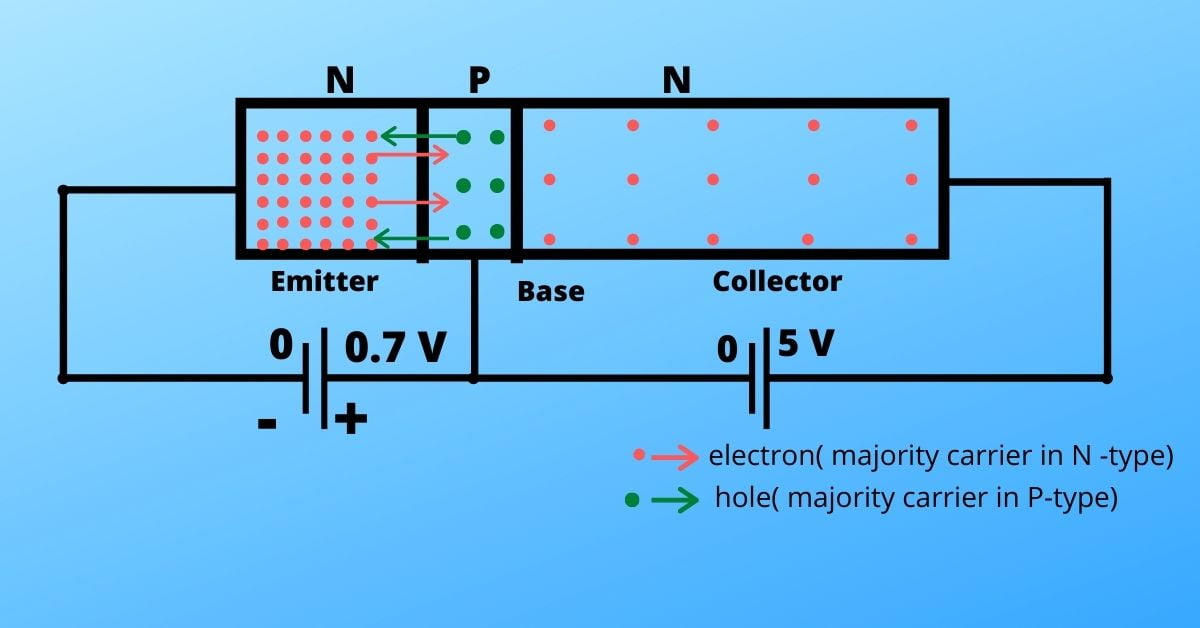
After electrons reach the base from the emitter the electrons can either go through the base region terminal or they can go through the collector region terminal to complete the circuit.
If you have a little idea or if you have read any articles about transistors, you may wonder why I am not giving the doping profile and width of regions till now. This is because this portion of the post is ideal to understand those things.
Now if you want current through the base region then the electrons must go through recombination. But to use a transistor properly we need to collect the electrons through the collector region. For this, we have to reduce the recombination process. This solution can be achieved by two things- first, lower the doping in the base region and second, by reducing the width of the base.
When the electrons reach the base (P-side) it becomes a minority carrier (for NPN transistor). So if you make the collector-base junction Forward bias, there is almost no chance that the electrons can cross the barrier.
But if you make the collector-base junction reverse-bias, electrons (as they are minority carriers in the base region for P-type semiconductor) can easily cross the junction and can be collected through the collector.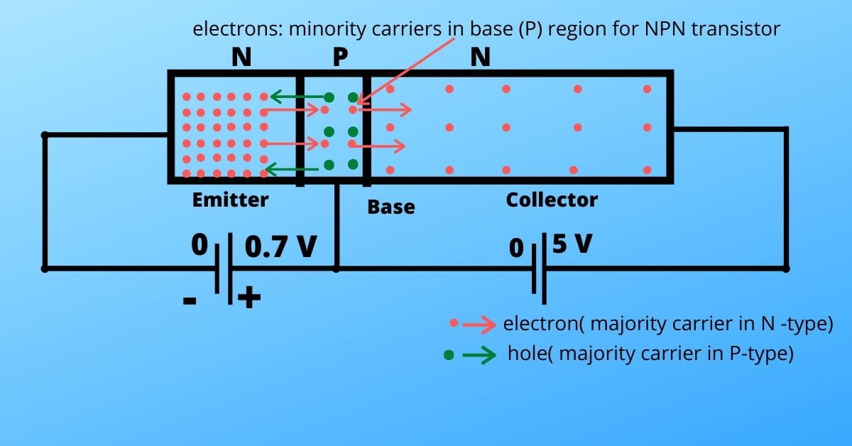
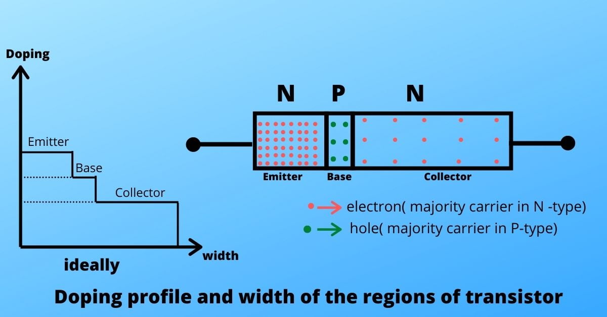
Doping Profile and Width of the regions
- Emitter: Emitter’s work is to emit electrons at a large number. So it is heavily doped. To dope something heavily it is better to maintain the width small to moderate.
- Base: As discussed earlier, the base is made very thin and very lightly doped.
- Collector: This region is made large to overcome the thermal issues raised by the operation of the transistor. The doping of the collector region depends on the uses of the device. Sometimes the collector is made larger than the base and sometimes doping is smaller than the base.
Understanding the Circuit Symbol
As you know, there are three terminals in a transistor.
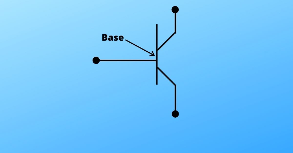
The middle portion can be easily identified as the base but it is hard to tell the difference between emitter and collector just by looking at the figure.
So to identify the emitter, we always put an arrow mark on the emitter. It is also possible to tell whether the transistor is NPN type or PNP type by seeing the direction of the arrow on the emitter.
We know that the direction of current is always opposite to the flow of electrons and towards the flow of holes.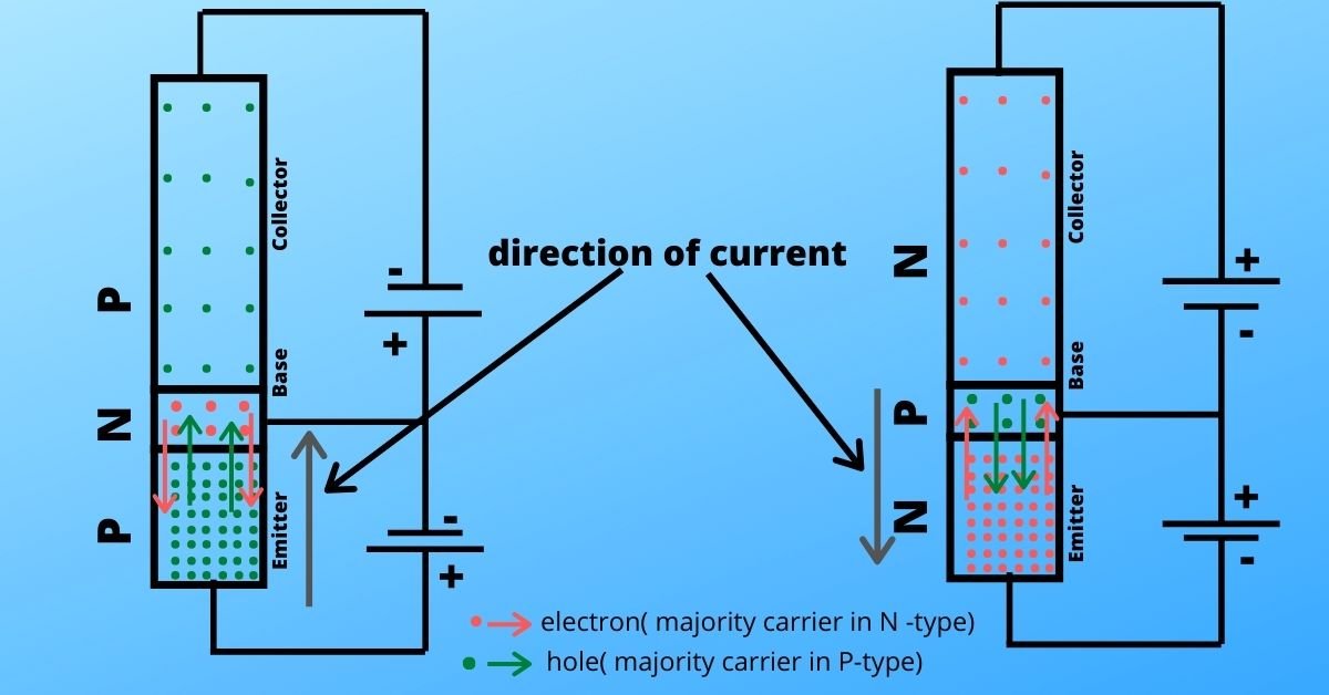
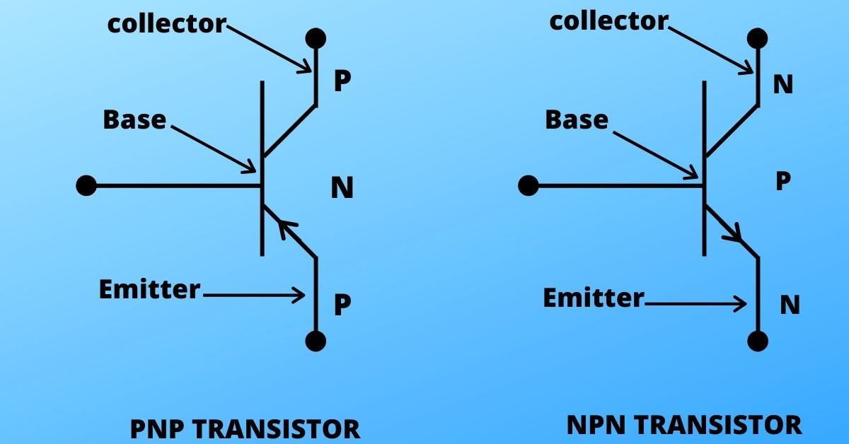
If you are still facing confusion to identify the proper direction of the arrow of the emitter, you can go with this shortcut. Just draw the arrow in the direction from P to N and name them accordingly.
Current profile and parameters of transistors
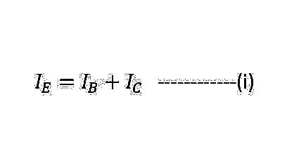
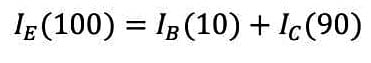
It can be proven that the emitter current (IE) is the sum of the base current (IB) and collector current (IC).
Okay, I hope you have understood the things till now. Here, I give you a pretty decent assumption to let you understand the different parameters.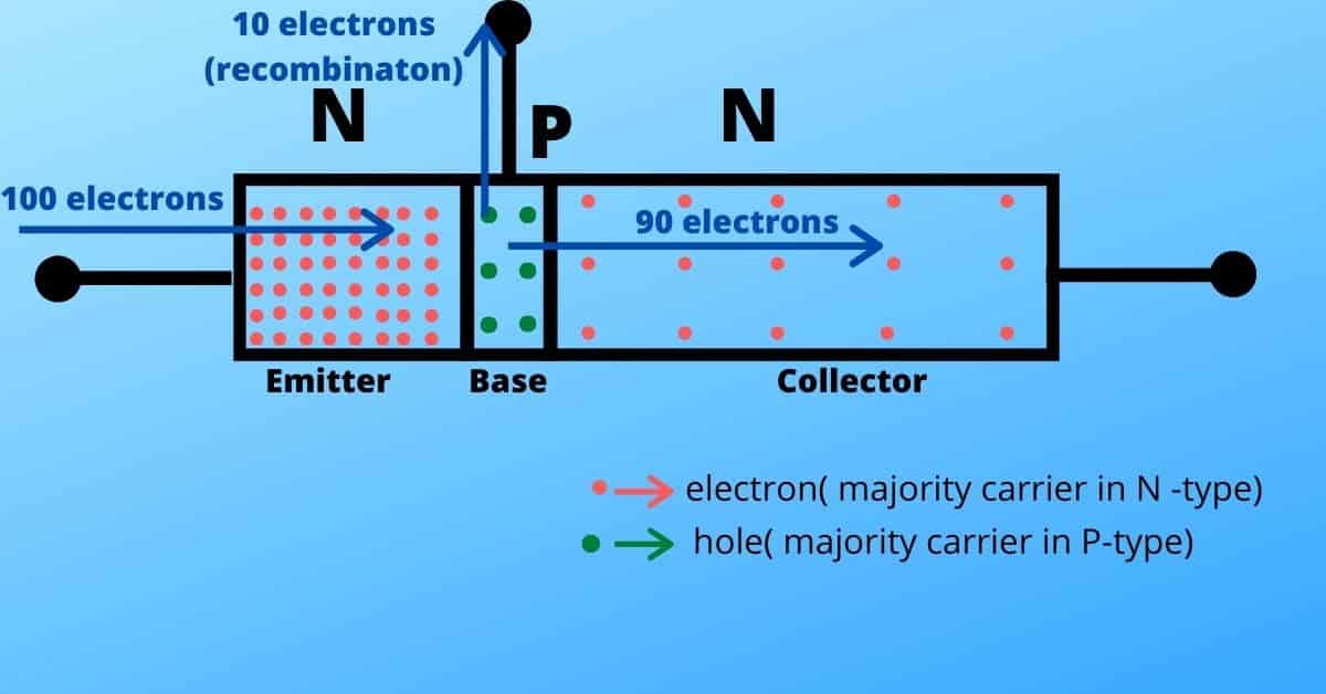
Look at the above diagram. Say, 100 electrons are injected from the emitter to the base (here I take 100 electrons to simplify the calculations and understanding). Out of 100 electrons, 10 electrons participate in the recombination process and 90 electrons are collected through the collector region. Now, see those numbers carefully and you find the similarity with equation (i) between them.
This is not the end, there are a lot more things to understand. From this point, try to think reversely. If 20 electrons emit from the base instead of 10 electrons, the number of electrons emitted from the emitter and collected through the collector is also changed to hold the equation (i). In this way, we can control the number of electrons collected through the collector.
We will stick with the previous example a bit more. We have, 100 electrons emitted from the emitter, 20 electrons collected through the base. So we can say, collected electrons are 80% of the emitted electrons.
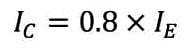
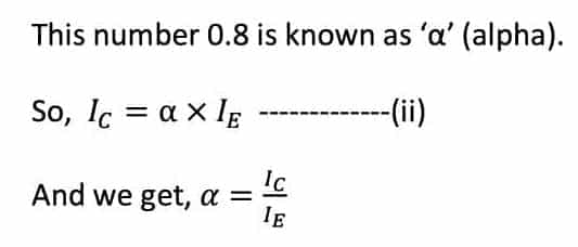
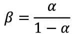
The value of alpha has a maximum value of 1 (ideally). Generally, a good transistor has an alpha value very close to 1 as the higher value of alpha means a greater number of electrons collected through the collector. It is the basic technique of amplification. Value of alpha depends on the doping concentration, width of the regions, etc.
There is another relation between Input (Ib) and output (Ic). The ratio of Ic and Ib is called Beta.
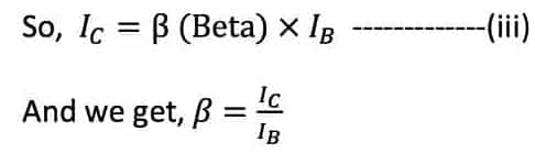
Beta is the factor which indicates how much the output current is amplified and it is also called as ‘Current gain’. Normally, Beta has a much higher value than alpha (say 500 or 800 and so on).
The relation between alpha and beta
This much in this post; for characteristics and use please see our post on characteristics and uses of transistors.
If you have any query regarding this post, don’t forget to comment below. Thank you.
What do you mean by the word “transistor”?
A semiconductor device in which a layer of semiconductor is sandwiched between two layers of another type of semiconductor.
What are the fabrication techniques that are used to build a transistor?
Grown junction technique, Alloy junction technique, Diffusion technique, Epitaxial technique.
What are the types of the transistors depending on use of semiconductor?
two-i)NPN , ii)PNP .
How many regions are there in a transistor?
3 regions- i)Emitter, ii)Base, iii)Collector.