The p-n junction diodes are one of the most used elements in electronic circuits. It is a non-linear, active element. For a definite polarity, it conducts well but becomes non conducting with opposite polarities. This property is quite similar to the property of vacuum diodes. Hence, the p-n junction is called a semiconductor diode. Semiconductor diodes are widely used in the large group of semiconductor devices.
What is a semiconductor?
A semiconductor is basically a solid whose electrical conducting property lies somewhere between the conductivity of metals and the conductivity of insulators.
The most commonly used semiconductors are-
- Silicon
- Germanium
Different types of semiconductor
Intrinsic semiconductor
Pure semiconductor solids in their natural form meaning no impurities mixed with them are called intrinsic semiconductors.
In this type of semiconductors, electrical conductivity increases very slowly with respect to temperature. In absolute zero the electrical conductivity is zero.
Extrinsic semiconductor
When a small amount of trivalent or pentavalent impurity is doped in a pure semiconductor, then it is called extrinsic semiconductor.
In this type of semiconductors, electrical conductivity increases rapidly with respect to temperature.
There are two types of extrinsic semiconductors:
P-type semiconductors
If a small amount of pentavalent impurity is doped in the pure semiconductor crystals, the conductivity increases significantly. This type of semiconductors are called p-type semiconductors. Here, majority carriers are holes and minority carriers are electrons. Immobile charge carriers are the acceptor impurity as the impurity atoms accept electrons from the crystal.
For example, if Aluminium (Al) (trivalent) is doped in intrinsic semiconductors (pure Silicon/ Germanium) then the mixture will be the p-type semiconductor.
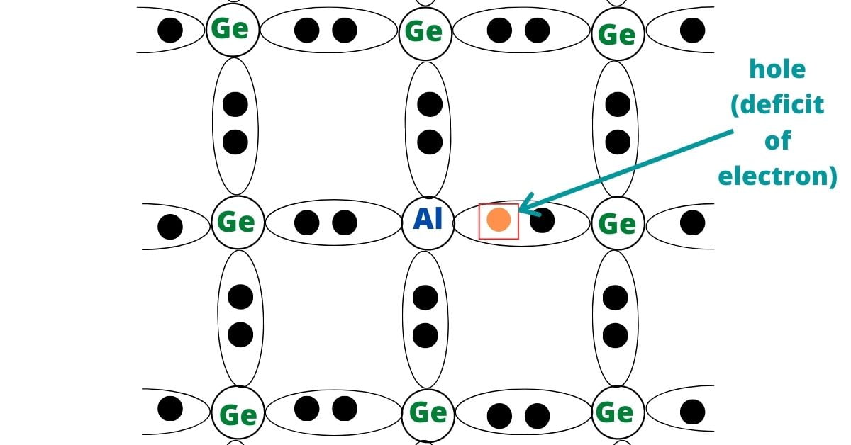
‘Al’ has three valence electrons which make three covalent bonds with Germanium’s three valence electrons out of four electrons. So there is always a deficiency of an electron to form the fourth covalent bond from the Aluminum side. The deficit of the fourth electron creates a hole.
N-type semiconductors
If a small amount of trivalent impurity is doped in the pure semiconductor crystals, the conductivity increases significantly. This type of semiconductors are called n-type semiconductors. Here, majority carriers are electrons and minority carriers are holes. Immobile charge carriers are the donor impurity as the impurity atoms donate electrons from the crystal.
For example, if Arsenic (As) (pentavalent) is doped in intrinsic semiconductors (pure Silicon/ Germanium) then the mixture will be the n-type semiconductor.

Arsenic has five valence electrons which make four covalent bonds with Germanium’s four valence electrons. So there is always an extra free electron from the Arsenic side.
What is a p-n junction diode?
When one side of a single crystal of a semiconductor is doped with p-type impurity and the other side of the same crystal doped with n-type impurity a p-n junction is formed.
Can we form a p-n junction just by putting p-type and n-type impurities side by side?
The answer is no, as the lattice structure remains discontinuous in the system they do not act like a p-n junction.
Why is the p-n junction diode called a ‘semiconductor diode’?
A p-n junction diode conducts when the applied voltage has the same polarity, but it is non-conducting for the opposite polarities. Thus, a p-n junction is called a semiconductor diode.
Fabrication techniques
There are four basic techniques to form a p-n junction diode-
- Grown junction techniques.
- Alloy junction techniques.
- Epitaxial techniques.
- Diffusion techniques.
What is the Potential barrier? How does it develop?
After the formation of the junction, there is an event of immediate diffusion due to thermal agitation. Some holes from p-side diffuse into n-side and some electrons from n-side diffuse into p-side.
Hence, a deflection region is formed. Its width covers the equal portion of each side. This deflection region contains immobile charge carriers as all the mobile charges diffuse on both sides. Thus, the presence of immobile charges creates a potential difference across the junction, this potential difference is called the potential barrier.
Why is the voltmeter unable to read the potential difference?
In the junction of the p-n junction diode, there exist only immobile charge carriers. If a voltmeter is connected in the deflection region no charge will flow through the connecting wire. Thus voltmeter is unable to read the barrier potential.
Different types of p-n junction diode
There exists a variety of p-n junction diodes, some of them are-
- Ordinary p-n junction diode
- Zener diode/Breakdown diode
- Light emitting diode(LED)
- Photodiode
- Schottky diode
- Varactor diode
- Tunnel diode
- Switching diode
- Backward diode
- p-n junction laser
- Solar cell.
Biasing of p-n junction diodes
When a dc voltage is applied across the p and n section of the p-n junction diode, then it is called ‘Biasing’. There are basically two types of biasing-
- Forward biasing
- Reverse biasing
Forward biasing
If the external voltage is applied across the p-n junction in such a way that p-side is connected with the positive terminal and n-type is connected with the negative terminal, then this biasing is called forward biasing.
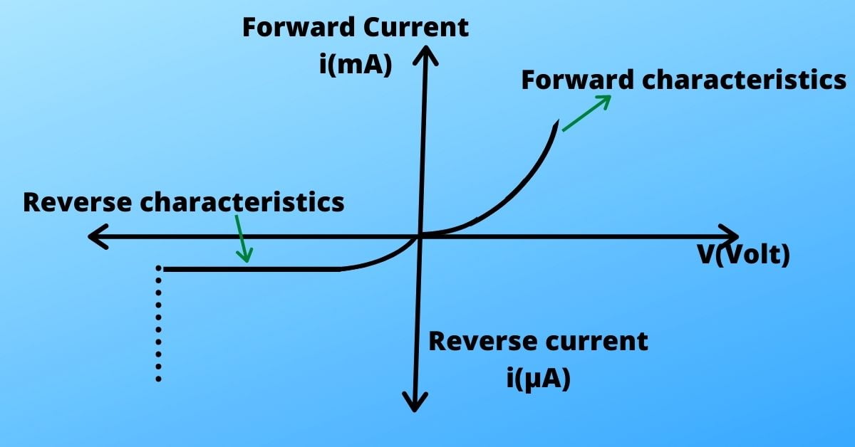
In this scenario, holes from p-side diffuse into n-side as well as electrons from n-side diffuse into p-side. Thus, the width of the potential barrier is reduced and the current is flowing from p to n region of the junction. This current is called forward current. The forward current increases exponentially with the applied voltage.

Reverse biasing
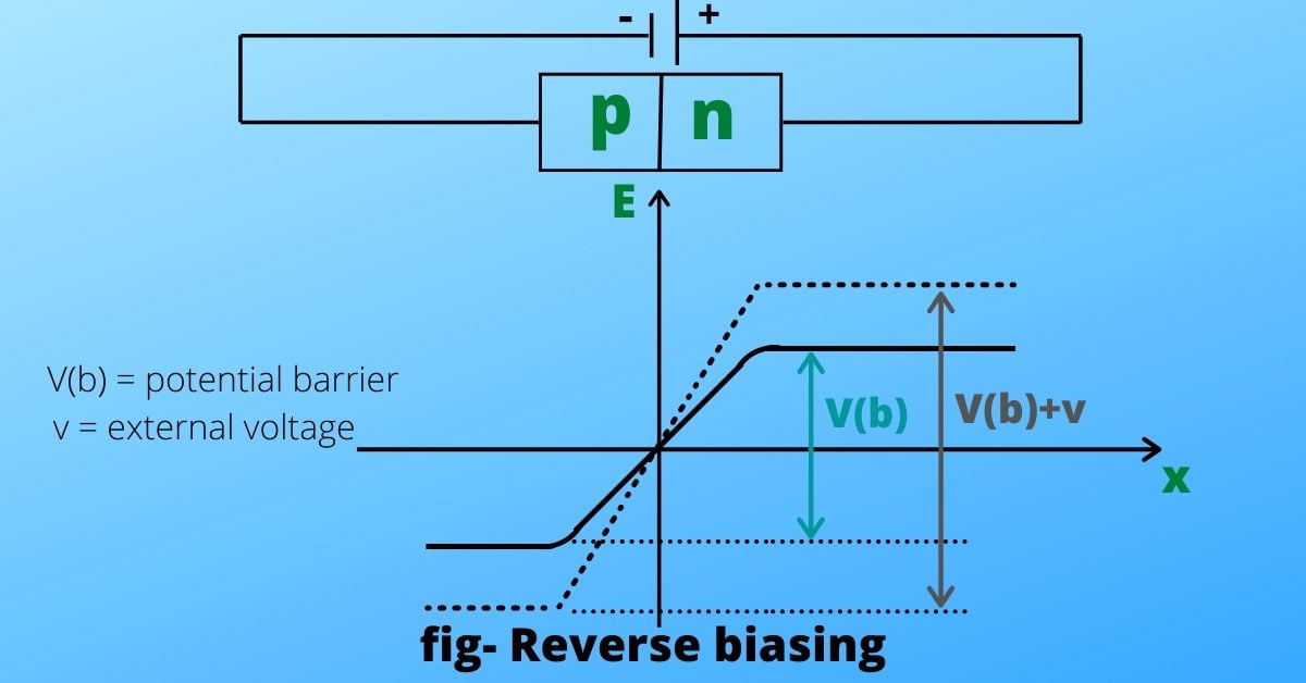
If the external voltage is applied across the p-n junction in such a manner that the p-side is connected with the negative terminal and n-type is connected with the positive terminal, then this biasing is called reverse biasing.
Thus majority carriers are unable to overcome this extended potential barrier. But the minority carriers (electron from p-side and hole from n-side) can cross the junction. This flow of minority carriers results in a small amount of current(generally in micro Ampere range). This current is known as Reverse Bias Saturation Current. Reverse Bias Saturation Current is independent of the applied reverse voltage.
V-I CHARACTERISTICS
Resistance
- What is Static Resistance?
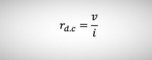
The ratio of voltage and current of a diode is defined as Static or dc resistance. As the diode has non-linear characteristics, its static resistance varies with current.
- What is dynamic Resistance?
In case of small-signal operation, the current flowing through a diode varies with some dc operating current. The resistance offered by the diode to this varying current is known as Dynamic resistance.

Capacitance
There are two types of capacitance –
- Transition region or barrier region capacitance: When a reverse bias is applied across the p-n junction the width of the depletion region is increased. Thus the number of immobile charges will also increase. This increase of immobile charges may be considered as a capacitance effect.
For dV voltage change if the change in charge is dQ then, the incremental capacitance,
What is an abrupt or step graded junction?
Using alloy junction technique step graded junctions are made. There is an abrupt change from p-type to n-type impurity in step graded junctions.
What is a linear graded junction?
Using Grown junction technique linear graded junctions are formed. The space charge density changes linearly with distance.
- Diffusion Capacitance: The concentration of injected charges in the junction region is changed with the variation of Forward bias voltage. This may be considered as a capacitance effect, called Diffusion capacitance.
Charge Storage Phenomena
If a diode in forward bias is switched rapidly to reverse bias, the charge Storage Phenomena occurs. The concentration of minority carriers is more in forward bias than reverse bias in the junction region. When the system is put into reverse bias, the diode current does not change immediately. This is because of the time taken by the excess carriers to move from forward to reverse bias. Hence there is a few microsecond delay to fall its steady-state reverse voltage value. This phenomenon is called charge Storage Phenomena. It is also a drawback of semiconductor diodes as it can not be used in the higher frequency range.
Use
- Diodes are used to make rectifiers to separate ac and dc components.
- Diodes are used to make filters.
- Voltage multipliers are also made with diodes.
- Zener diodes are used to make voltage regulators.
- Light Emitting Diode (LED) can produce light.
These are some uses of diodes. There are several other uses of different types of diode.
what do you mean by a “semiconductor”?
A semiconductor is basically a solid whose electrical conducting property lies somewhere between the conductivity of metals and the conductivity of insulators.
how a p-n junction diode is formed?
When one side of a single crystal of a semiconductor is doped with p-type impurity and the other side of the same crystal doped with n-type impurity a p-n junction is formed.
what is forward biasing?
If the external voltage is applied across the p-n junction in such a way that p-side is connected with the positive terminal and n-type is connected with the negative terminal, then this biasing is called forward biasing.
what is reverse biasing?
If the external voltage is applied across the p-n junction in such a manner that the p-side is connected with the negative terminal and n-type is connected with the positive terminal, then this biasing is called reverse biasing.

