In our previous post, we learnt about the mechanism and different parameters. If you missed it please check our ‘ A to Z about transistor‘ post first for better understanding. In this post, we will discuss about the different characteristics of transistors and their uses. So let’s get into it.
Different modes
There are three different configurations or modes depending on common (ground) terminal connection-
- Common Base configuration or CB mode.
- Common Emitter configuration or CE mode
- Common Collector configuration or CC mode.
CE mode is superior over the other two modes. In this post, we discuss and understand the characteristics of the transistors and their uses particularly in CE mode.
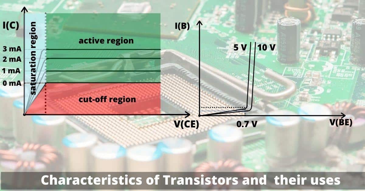
Different Characteristics of transistors
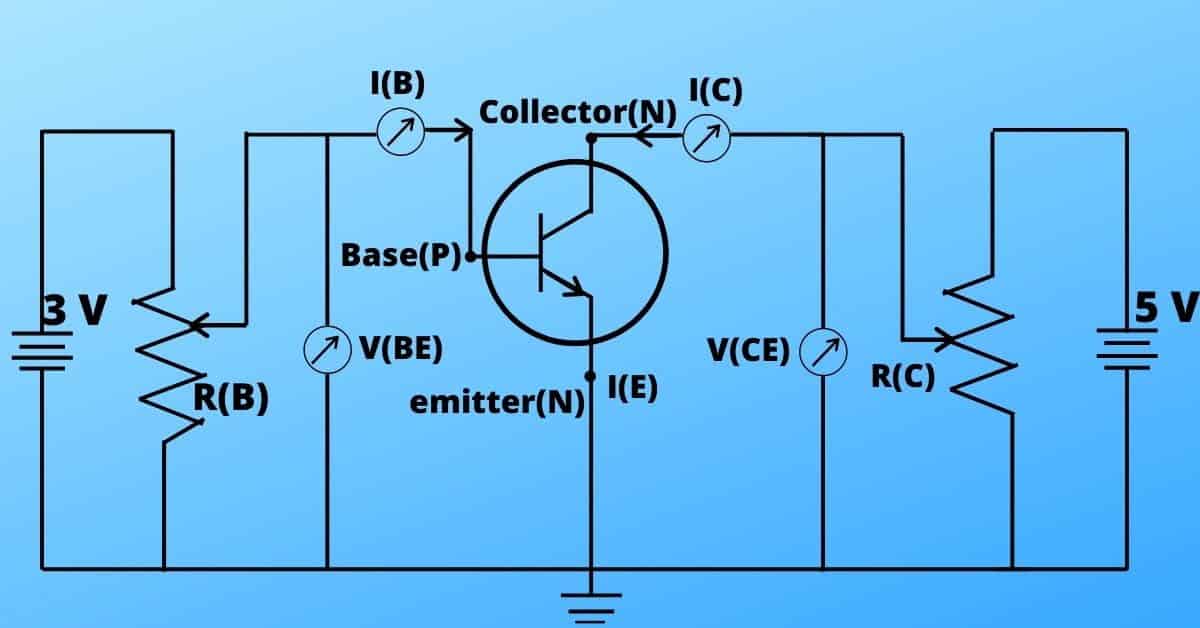
When a transistor works as an amplifier, it’s base terminal works as input terminal and collector terminal works as an output terminal. So, for the base terminal, the current-voltage relationship is known as input characteristics. Similarly, the collector terminal, the current-voltage relationship is known as output characteristics.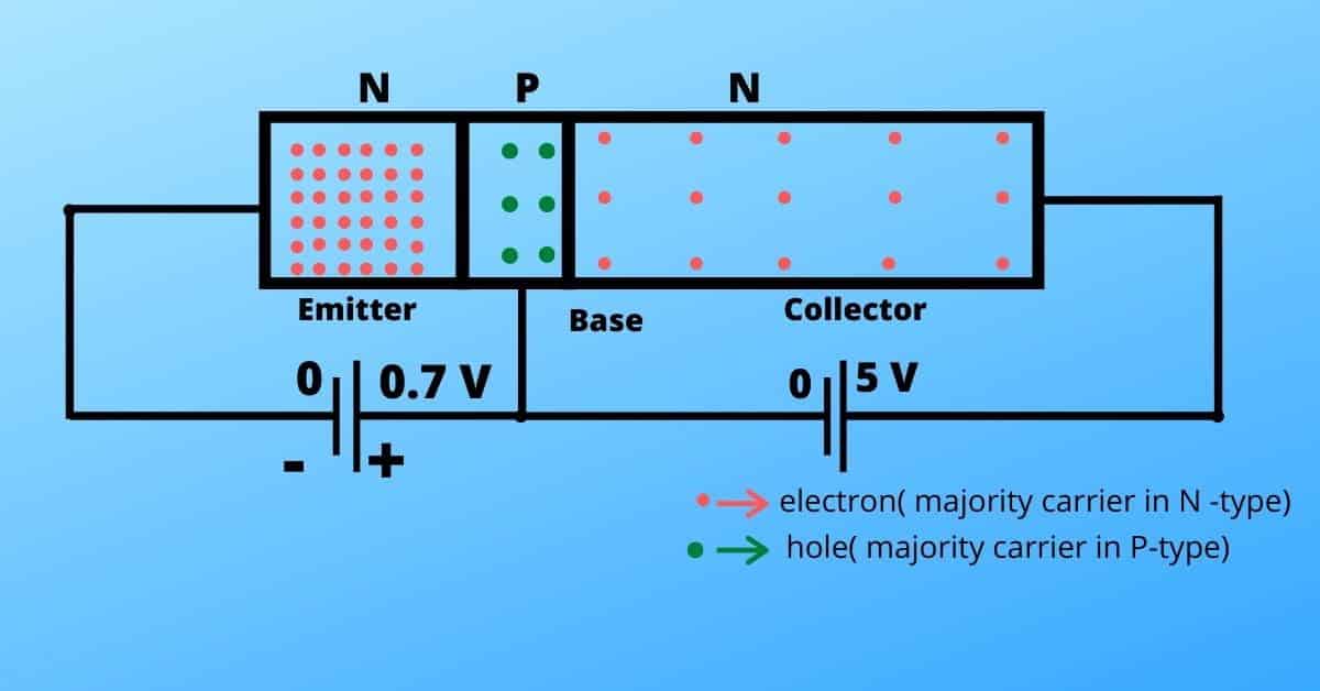
The base voltage is denoted as V(BE) meaning the base voltage has a value with respect to the emitter(ground).
The collector voltage is denoted as V(CE) meaning the collector voltage has a value with respect to the emitter(ground).
Input characteristics of transistors
The graph between V(BE) vs I(B) is called input characteristics of transistors for a constant value of V(CE). V(CE) is kept constant as it may affect the input current I(B).
The V(BE) vs I(B) graph is almost similar to p-n junction’s V-I characteristics graph for forward bias.
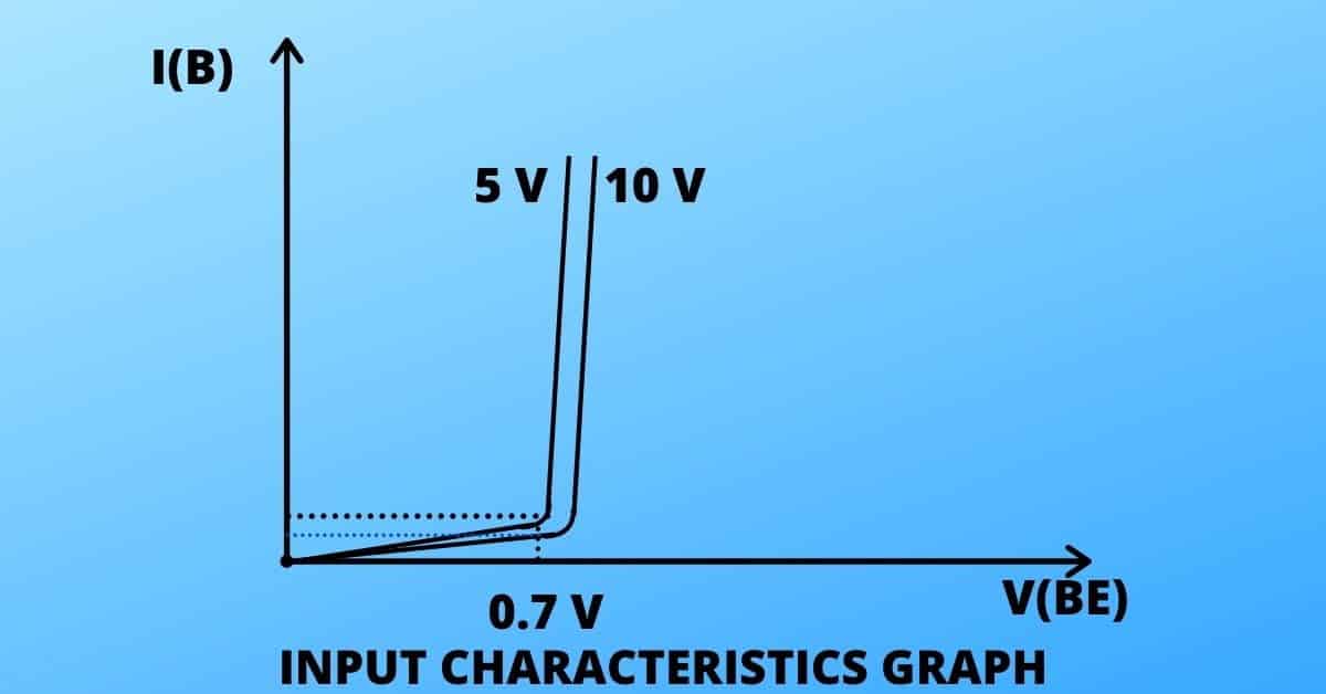
This is an ideal situation, but in reality, the collector voltage, V(CE) barely makes a considerable change in I(B).
Output characteristics of transistors
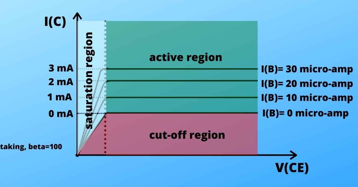
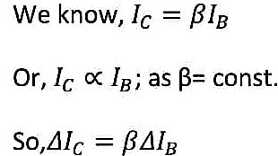
The graph between V(CE)vs I(C) is called the output characteristics of transistors for a constant value of I(B). As we know the I(C) has a dependence over I(B) [ if the value of I(B) doubles, the I(C) value also doubles].
The collector-base junction is kept in reverse bias. So the output characteristics graph is nothing but the graph of a p-n junction in reverse bias.
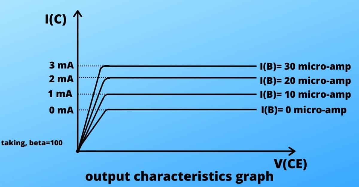
You can see that the initial portion of the graph is increasing gradually from zero to a certain extent and after that the graph is constant. The initial portion indicates if you reduce the collector voltage less than 0.7 Volt, the collector-base junction becomes forward biased. Thus it is very tough for minority carriers to flow from base to collector. Hence, you get almost negligible current until you hit 0.6- 0.7 volts.
Active, cut-off and saturation region
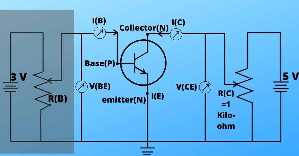
Case:1 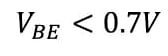
In this case, the depletion region does not vanish, so hardly any electrons are injected into the base. Therefore, hardly any electrons get collected through the base region.
( As no current flows through the transistor, there should be no voltage drop).
This stage is called the cut-off stage.
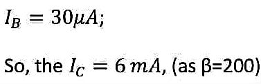
Case:2![]()
For 0.7 volts the depletion region vanishes, so the current starts flowing through the transistor. Let’s assume, the input current is 10 micro-amperes and current gain is 200 (i.e. beta=200).
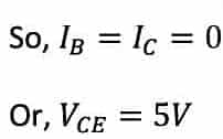
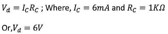
Now the voltage drop across R(C)(= 1 kilo-ohm) is,
And,
So, for
![]() , the transistor works as an amplifier.
, the transistor works as an amplifier.
This stage is called the active/linear stage.
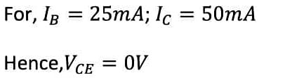
Case:3 ![]()
Let’s take
, .
.
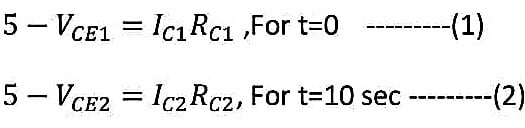
hence the voltage drop across R(C),
This is impossible as the voltage drop (6V) is higher than the supplied power(5V).
So, whatever changes you will do after 25 micro-ampere of input current, they do not increase the output current. The output current does not exceed more than 5 mA.
This stage is called the saturation stage.
Uses of transistor
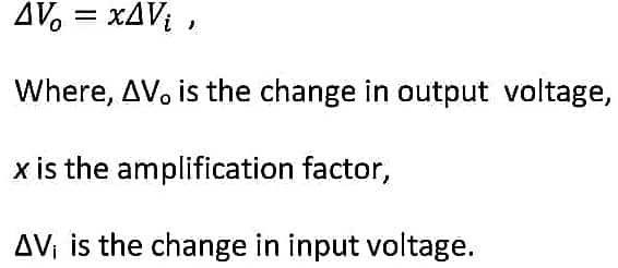
Voltage amplifier
Voltage amplifier is used to amplify the voltage using relationship-
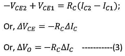
Now for collector region,
By subtracting equation (2) from equation (1), we get,
Similarly for the base region,
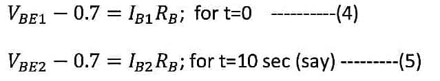
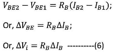
By subtracting equation (5) from equation (4), we get,
From equation (3) and equation (6) we get,
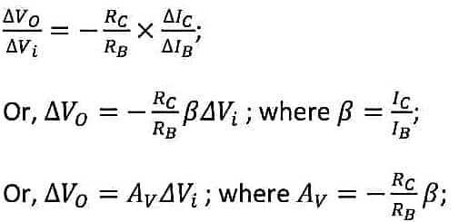
The term Av is called the voltage gain. The negative sign indicates that if the output voltage is increased then the output voltage is decreased by Av factor and vice-versa.
Transistor as a switch
The transistor has the cut-off region below 0.7 volts and saturation region for I(B)>25 mA .
For,
This is the condition for cut-off region.
For,
This is the condition for Saturation region.
So using these two regions we can make a switch. The Cut-off region can be considered as ‘off’ and the saturation region can be collected as ‘on’ like a conventional one.
Practical circuit example

When V(BE) <0.7 Volts, current does not flow through the transistor. So all the current flows through the LED and the LED turns on. This is the off mode.
When V(BE) =0.7 volt and I(B)>25 micro-ampere, the transistor is in saturation region and acts as a short circuit. So, no current will flow through the LED and it will not glow. This is the on mode of a transistor.
Advantages
- Unlike mechanical switches, these ones have no moving parts at all so it is more efficient and faster than a conventional switch.
- In modern days it is possible to build very tiny transistors so that they can fit inside a small IC in large numbers. Transistor can also do arithmetic calculations. These give a superior advantage to build different types of logic devices.
- A transistor can be operated as a switch with a small variation of voltage which makes it more convenient for use.
If you have any query regarding this post, please don’t hesitate to comment below. Thank you.
What are different modes of configuration?
Common Emitter mode or CE mode, Common Collector mode or CC mode, Common Base mode or CB mode.
What is the output characteristics graph?
The graph between V(CE)vs I(C) is called the output characteristics of transistors for a constant value of I(B).
What is the input characteristics graph?
The graph between V(BE) vs I(B) is called input characteristics of transistors for a constant value of V(CE). V(CE) is kept constant as it may affect the input current I(B).
What are the advantages of transistor switches over mechanical switches?
1.no moving parts, so efficient and faster; 2. possible to make in very small size which make it ideal for use in small logic devices like ICs; 3. can be used as a switch with a very small variation in voltage.